[測試] NVIDIA GeForce GTX 670出世,Kepler GK104家族群測大評比
NVIDIA Kepler GK104 大軍壓境好讀版
http://www.xfastest.com/forum.php?mod=viewthread&tid=76261&fromuid=38227
===============================================================================
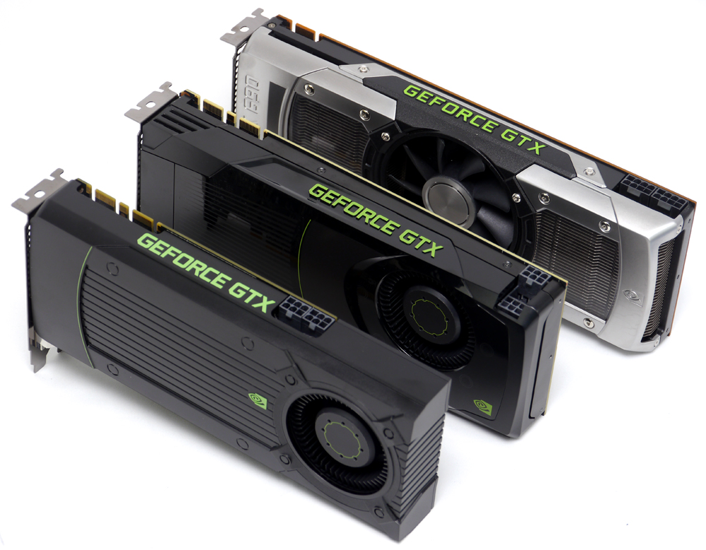
在經過NVIDIA GeFoece GTX 680和GTX 690旗艦級強大效能的洗禮之後,
Kepler架構開始往較超值的價位邁進。
以下我們除了探討Kepler GK104的小弟GTX 670之外,
另外也召集它的大哥們與競爭對手同步進行高階顯卡大評比!
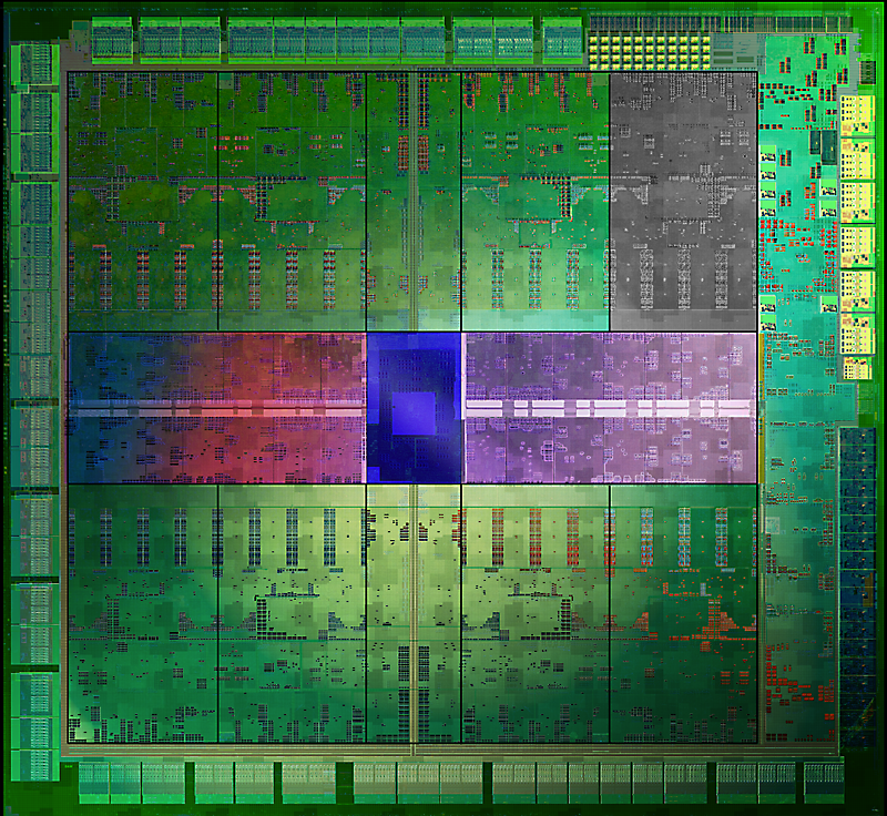
http://picx.xfastest.com/elvis/Graphic/NVIDIA/GeForce/GK104/01.jpg
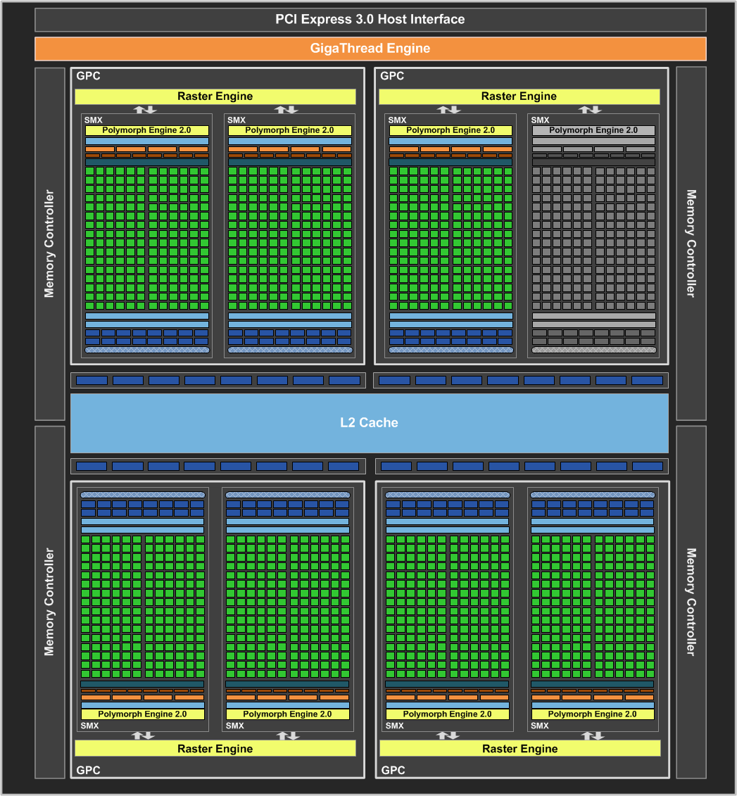
本次推出的GTX 670與它的大哥們同樣採用GK104晶片,但是與GTX 680相比,
GTX 670屏蔽掉一組SMX(Streaming Mulit-processor)單元,
因此CUDA Core總數從1536個縮減為1344個。
http://picx.xfastest.com/elvis/Graphic/NVIDIA/GeForce/GTX670/01.png
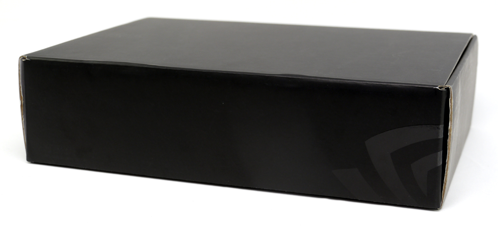
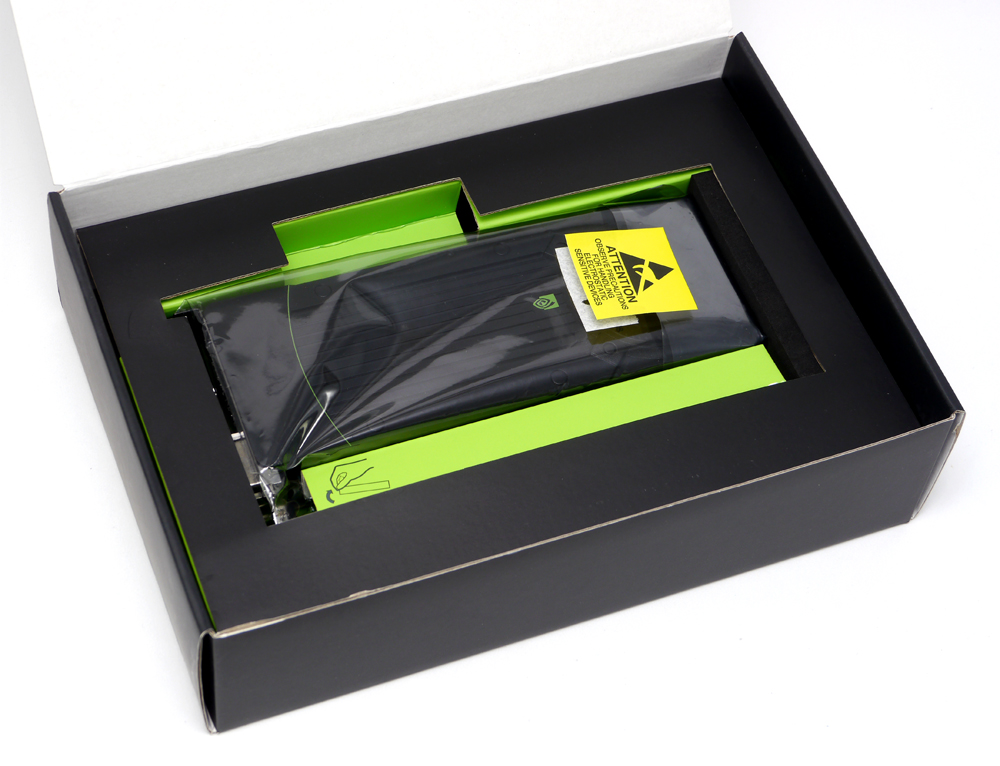
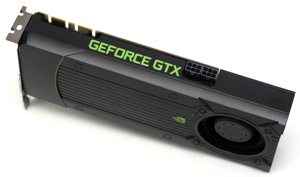
GTX 670 公版顯示卡參見
包裝方式與公版GTX 680相同
http://picx.xfastest.com/elvis/Graphic/NVIDIA/GeForce/GTX670/03.jpg
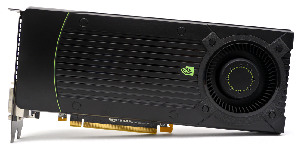
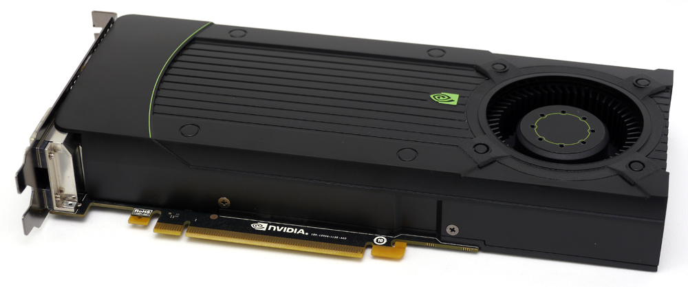
GTX 670 公版外觀與散熱
與GTX680類似,使用卡夾式的散熱器
http://picx.xfastest.com/elvis/Graphic/NVIDIA/GeForce/GTX670/06.jpg
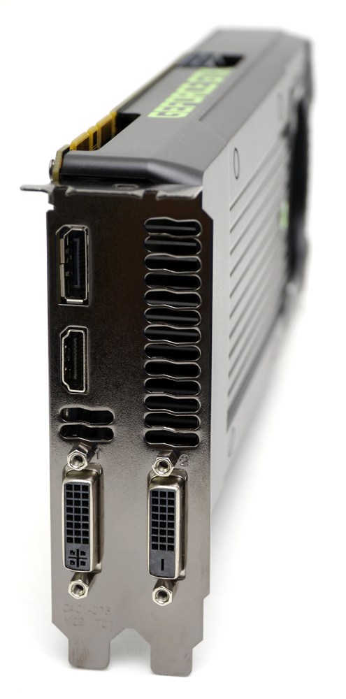
顯示輸出介面有DisplayPort 1.2、HDMI 1.4a、DVI-I與DVI-D
http://picx.xfastest.com/elvis/Graphic/NVIDIA/GeForce/GTX670/07.jpg
頂部可見綠色GEFORCE GTX印刷字樣以及兩組PCI-E 6 pin 12V電源輸入端子
http://picx.xfastest.com/elvis/Graphic/NVIDIA/GeForce/GTX670/08.jpg
傳輸介面也是採用最新的PCI-Express 3.0 x16
http://picx.xfastest.com/elvis/Graphic/NVIDIA/GeForce/GTX670/09.jpg
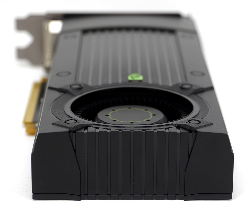
非常有意思的設計:散熱器長度比顯示卡PCB本體大上不少
http://picx.xfastest.com/elvis/Graphic/NVIDIA/GeForce/GTX670/11.jpg
鼓風式風扇葉片頂端使用圓框固定,減低運轉時扇葉的共振現象
http://picx.xfastest.com/elvis/Graphic/NVIDIA/GeForce/GTX670/12.jpg
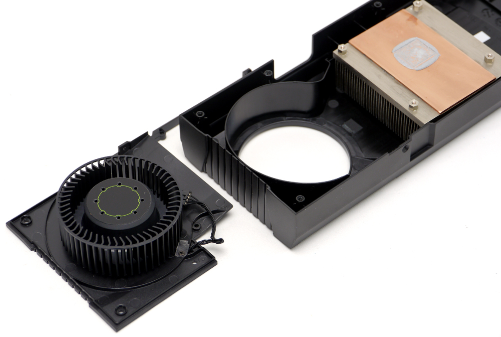
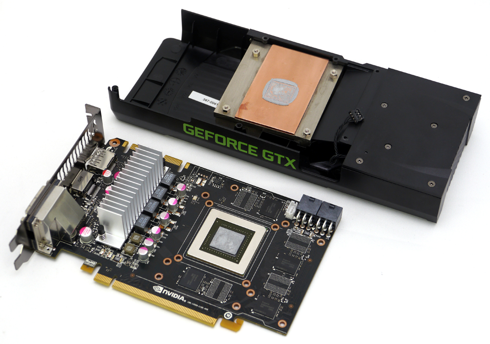
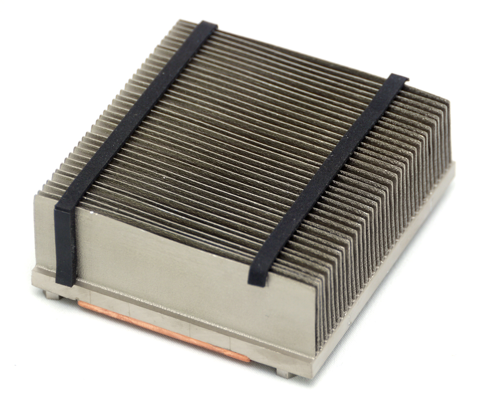
散熱模組與GPU的接觸面使用銅底,搭配封裝好的扁平式熱導管及鋁質鰭片
http://picx.xfastest.com/elvis/Graphic/NVIDIA/GeForce/GTX670/13.jpg
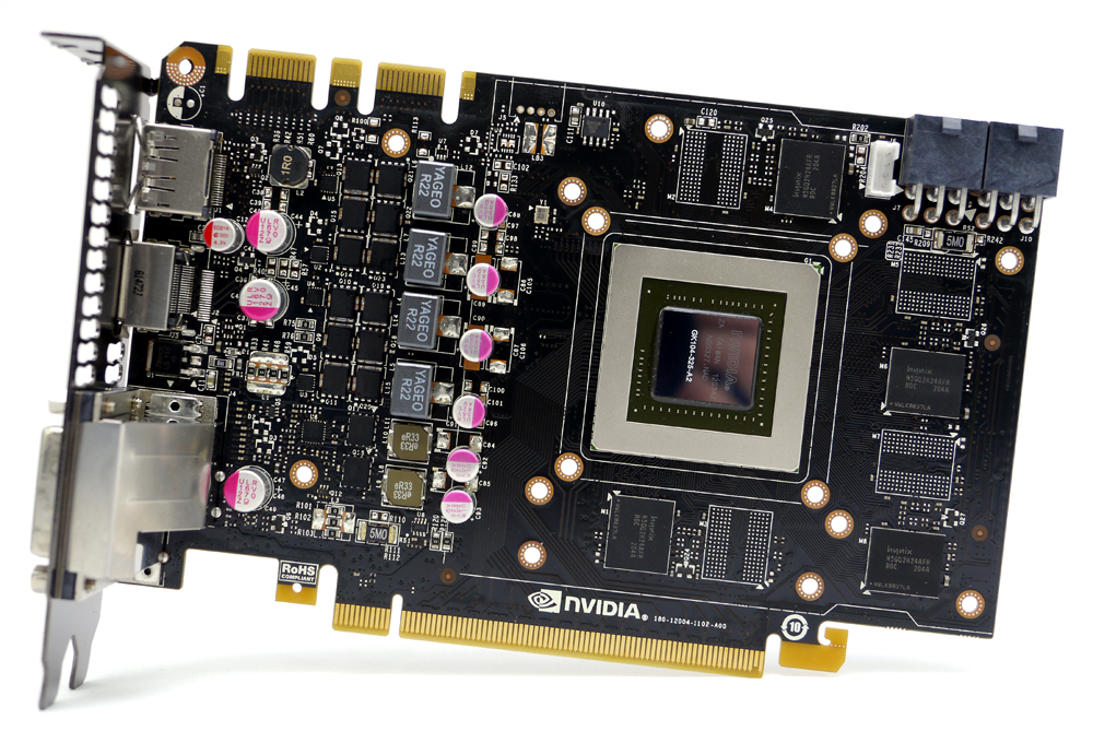
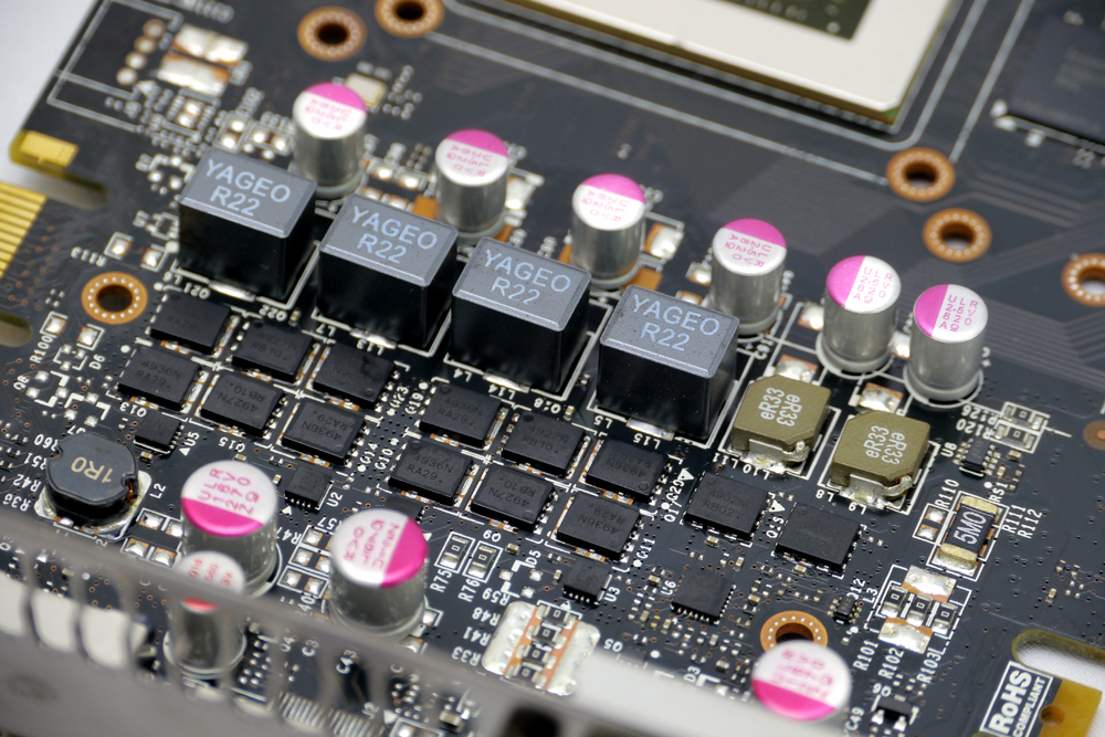
GPU使用4相供電,記憶體使用2相供電
http://picx.xfastest.com/elvis/Graphic/NVIDIA/GeForce/GTX670/15.jpg
GTX 670使用的晶片編號為GK104-325-A2
http://picx.xfastest.com/elvis/Graphic/NVIDIA/GeForce/GTX670/16.jpg
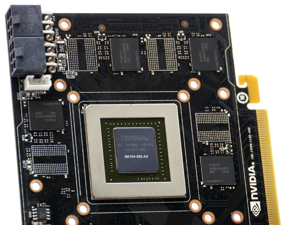
GDDR5顯示記憶體採用hynix H5GQ2H24MFR-R0C 2Gb的顆粒,正面用了4顆
PCB背面再用了4顆hynix H5GQ2H24MFR-R0C 2Gb顆粒,
前後共8顆構成2GB/256bit的容量介面
http://picx.xfastest.com/elvis/Graphic/NVIDIA/GeForce/GTX670/17.jpg
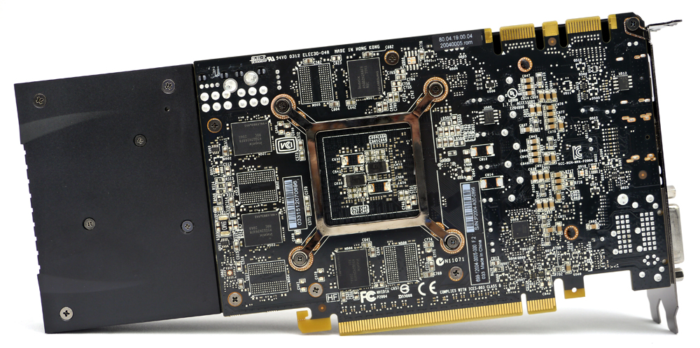
各位應該可以發現PCB前後還留存著各4個記憶體的空焊點,
因此可推論支援更高容量的記憶體
基本性能表現
測試平台與環境
http://picx.xfastest.com/elvis/Graphic/NVIDIA/GeForce/GTX670/18.jpg
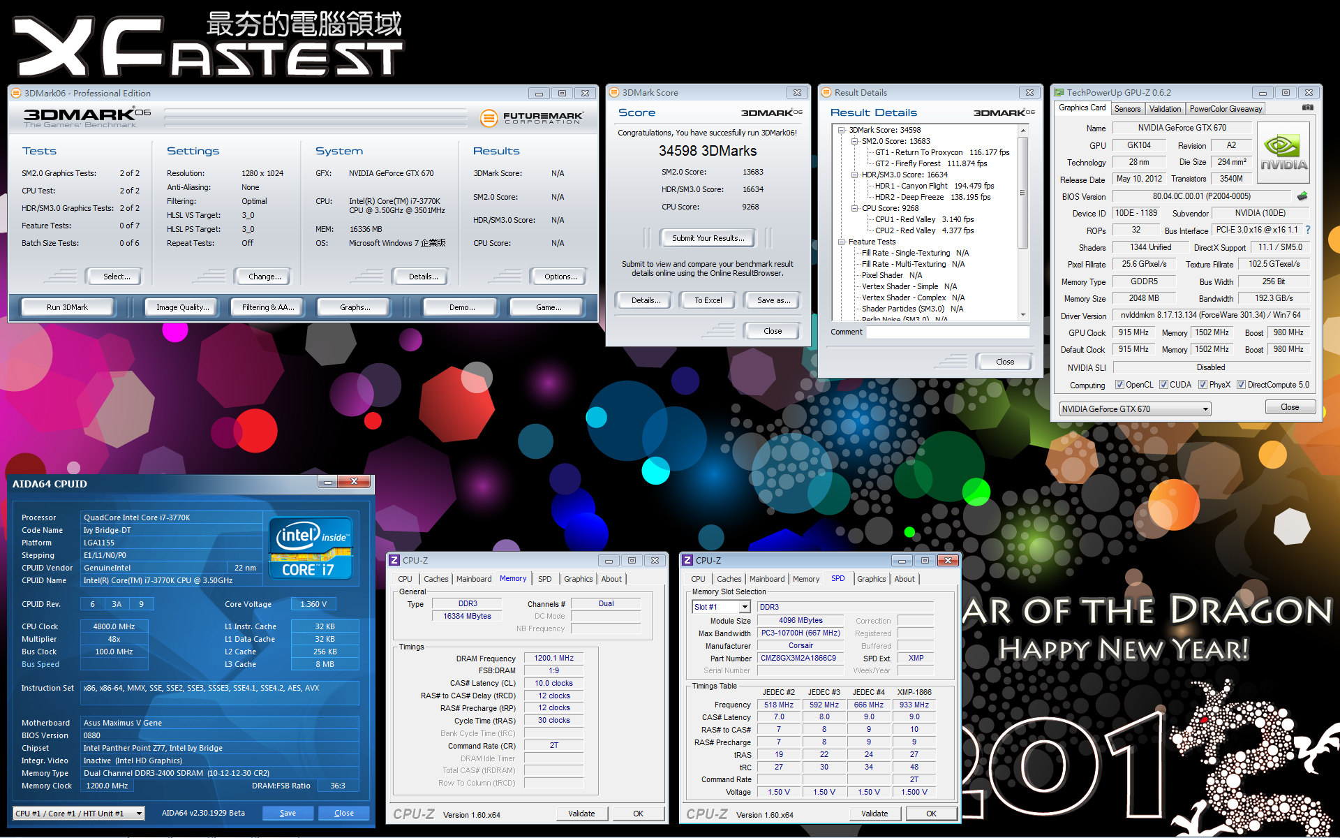
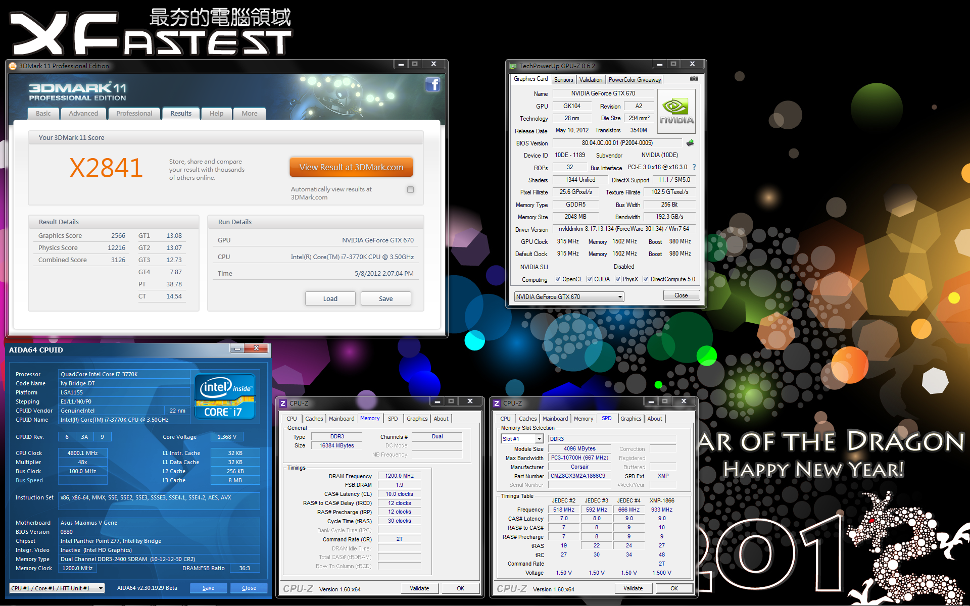
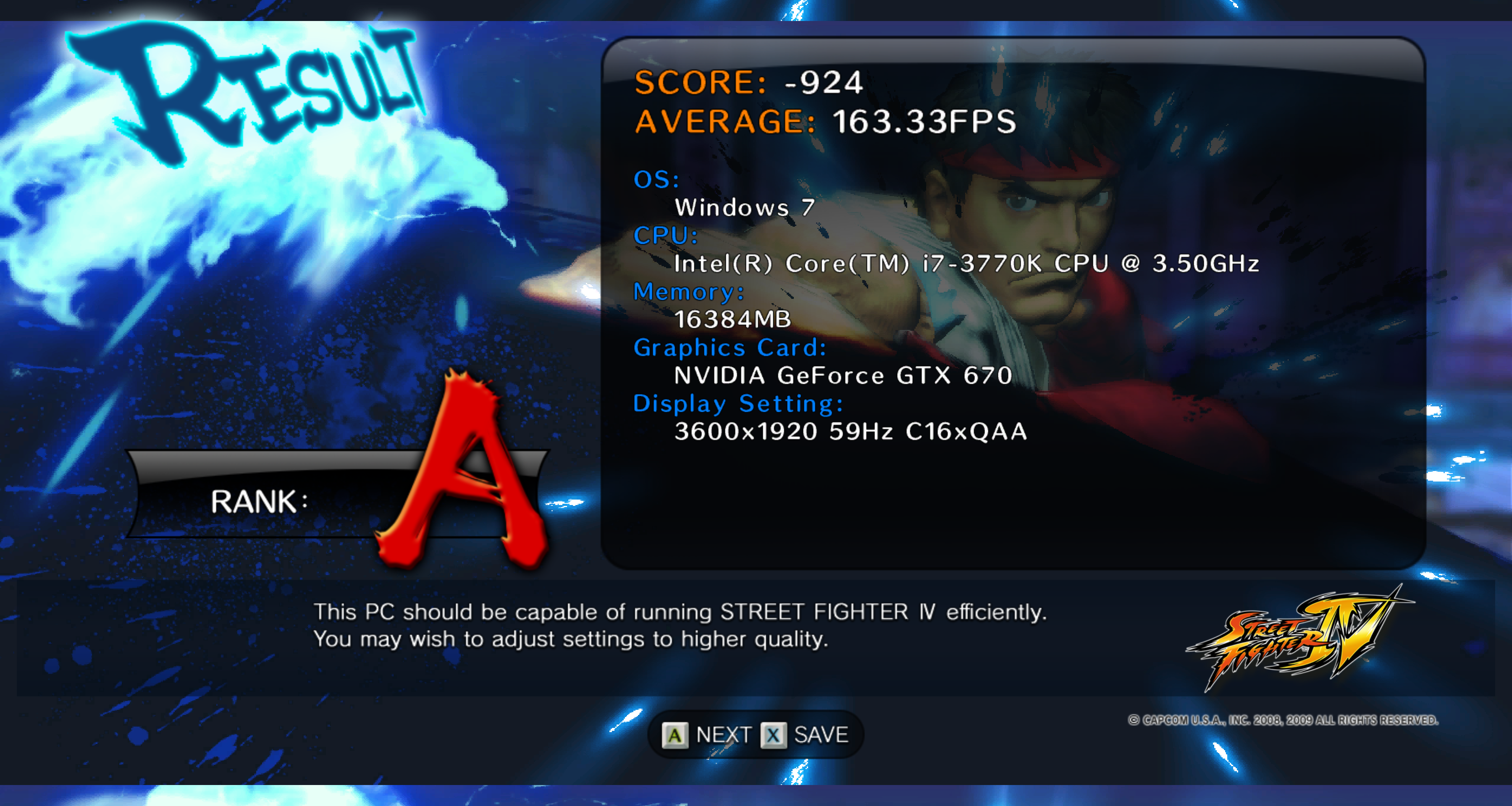
CPU: Intel Core i7-3770K Retail @ 4.8 GHz
Cooler: Antec KUHLER H2O 920 改裝2D冷排
Thermal Compound: Antec Formula 7
MB: ASUS ROG Maximus V Gene
RAM: Corsair Vengeance DDR3-1866 4GB*4 @ 2400 MHz 10-12-12-30-2T
Graphic: NVIDIA GeForce GTX 690
Storage: Plextor M3 SSD 256GB
PSU: Antec HCP-1200W
Chassis: Lubic Open Paltform 3
Monitor: Dell U2410
OS: Windows 7 64 Bit
GPU-Z
http://picx.xfastest.com/elvis/Graphic/NVIDIA/GeForce/GTX670/GPU-Z.png
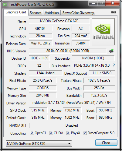
本次測試採用最新公布的301.34 WHQL版本驅動
3DMark06 (DirectX 9)
http://picx.xfastest.com/elvis/Graphic/NVIDIA/GeForce/GTX670/3DMark06.png
3DMark Vantage Performance (DirectX 10)
http://picx.xfastest.com/elvis/Graphic/NVIDIA/GeForce/GTX670/3DMarkVantageP.png
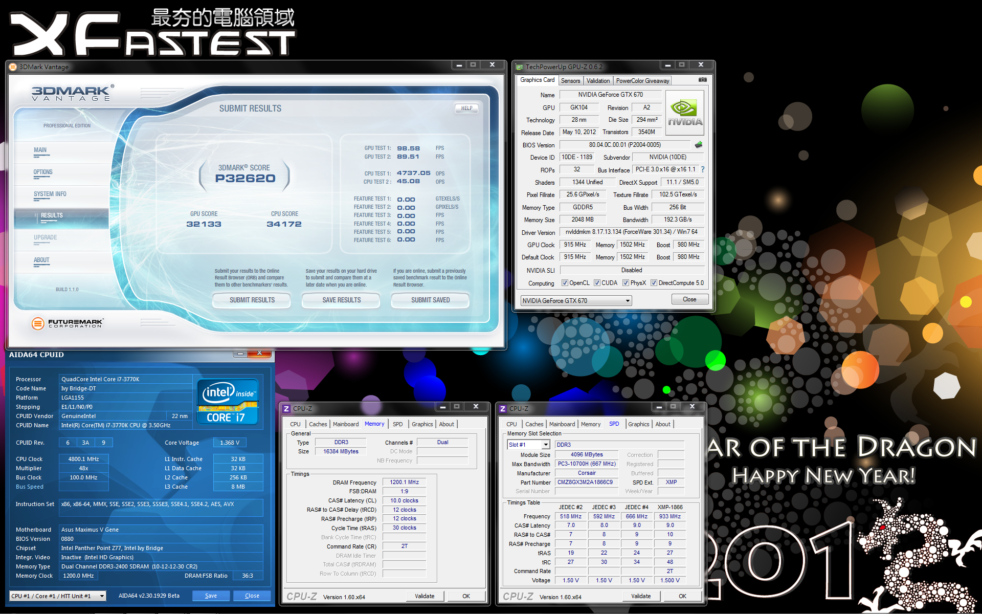
3DMark Vantage Extreme (DirectX 10)
http://picx.xfastest.com/elvis/Graphic/NVIDIA/GeForce/GTX670/3DMarkVantageX.png

3DMark11 Performance (DirectX 11)
http://picx.xfastest.com/elvis/Graphic/NVIDIA/GeForce/GTX670/3DMark11P.png

3DMark11 Extreme (DirectX 11)
http://picx.xfastest.com/elvis/Graphic/NVIDIA/GeForce/GTX670/3DMark11X.png
3螢幕高解析度性能表現
雖然是Kepler GK104家族的小弟,但GTX 670也是能夠單卡支援3+1螢幕輸出,
我們直接來看一下3螢幕玩遊戲加上特效全開時的性能表現吧~
快打旋風 4 (3600x1920, 16xQ CSAA, 特效全開)
http://picx.xfastest.com/elvis/Graphic/NVIDIA/GeForce/GTX670/StreetFighterIV.png
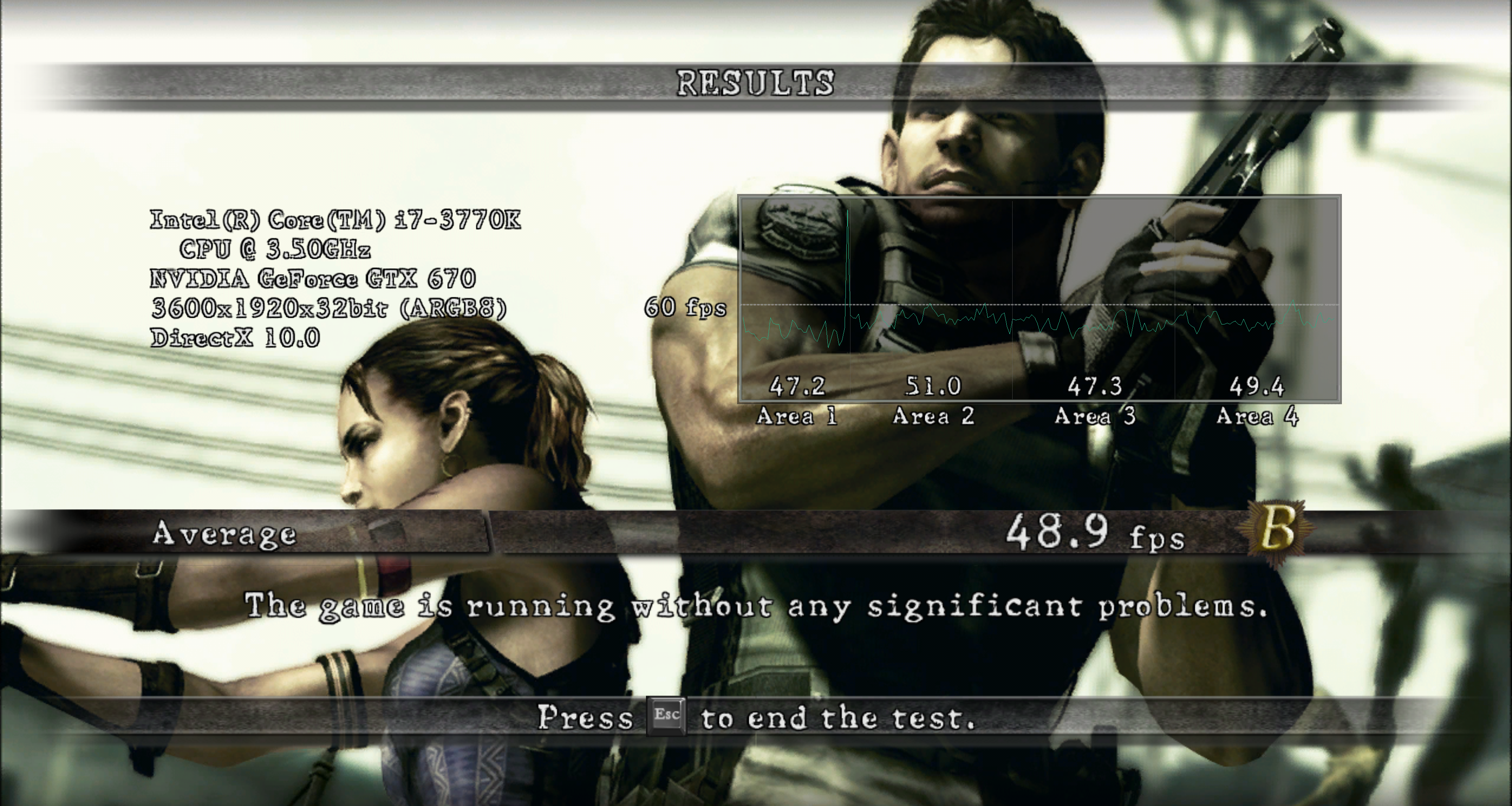
惡靈古堡 5 (DirectX 10, 3600x1920, 16xQ CSAA, 特效全開)
http://picx.xfastest.com/elvis/Graphic/NVIDIA/GeForce/GTX670/RE5.png
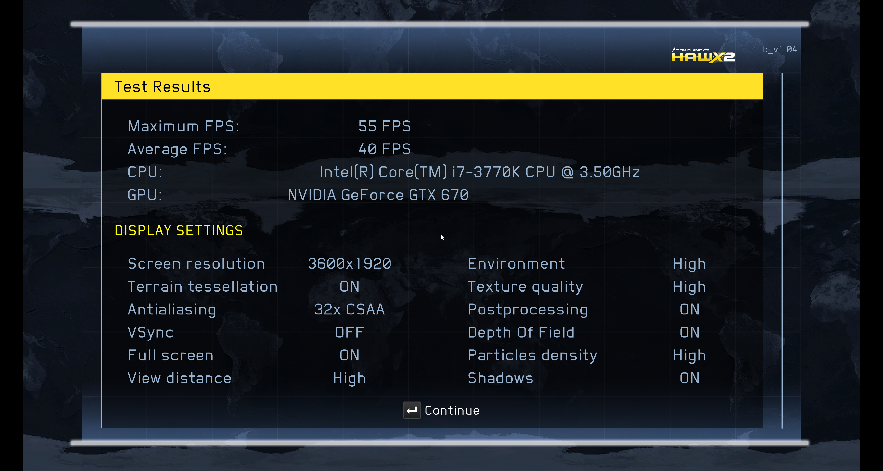
HAWX 2 (DirectX 11, 3600x1920, 32x CSAA, 特效全開)
http://picx.xfastest.com/elvis/Graphic/NVIDIA/GeForce/GTX670/HAWX2.png
越野精英賽:大地長征 3 (DirectX 11, 3600x1920, 8x MSAA, 特效全開)
http://picx.xfastest.com/elvis/Graphic/NVIDIA/GeForce/GTX670/DiRT3.png

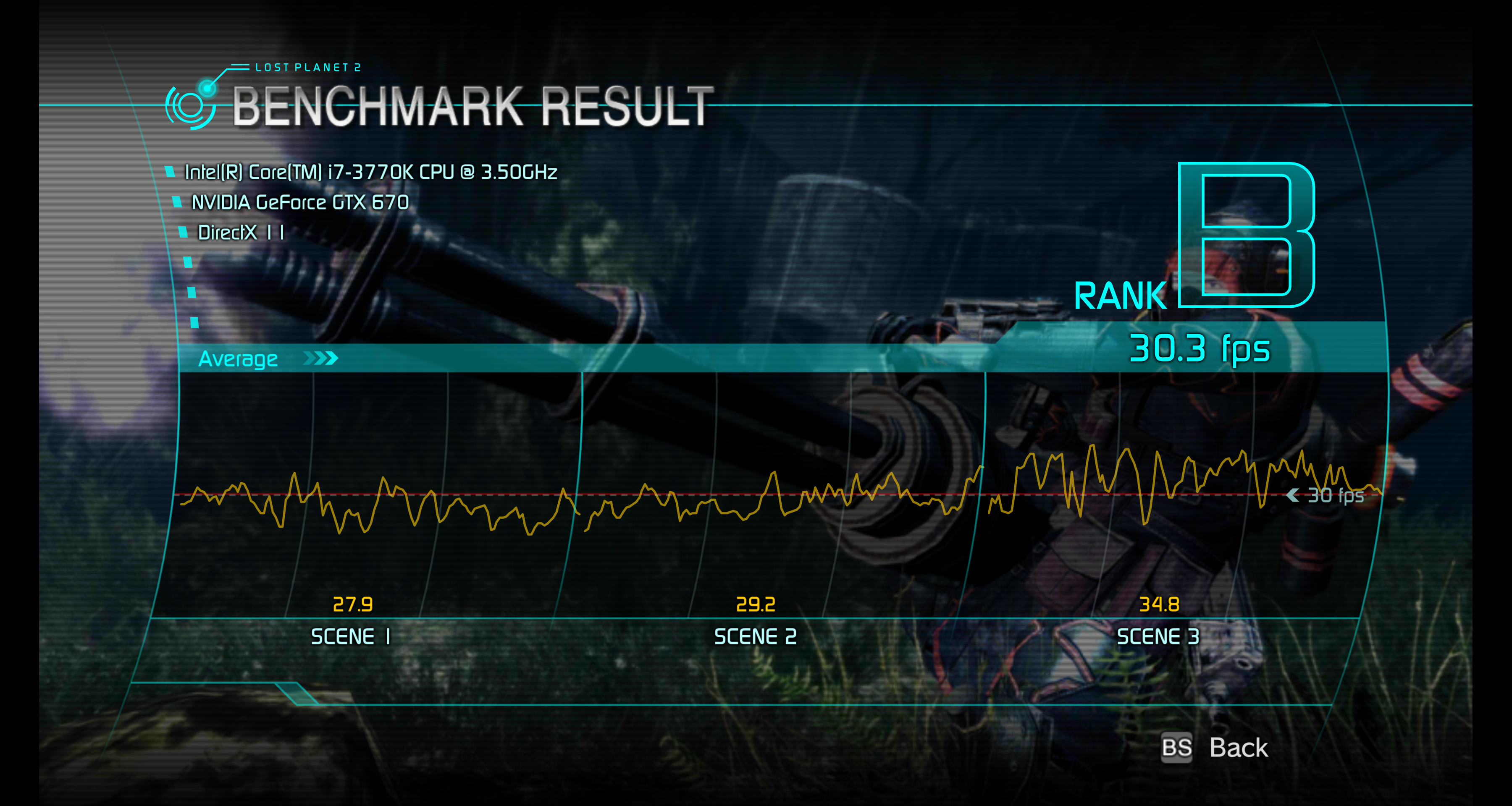
失落的星球 2 (DirectX 11, 3600x1920, 32x CSAA, 特效全開)
http://picx.xfastest.com/elvis/Graphic/NVIDIA/GeForce/GTX670/LP2.png
高階顯示卡性能功耗大車拚
測試平台與成績引用自XF顯示卡比較平台
http://www.xfastest.com/cms/VGA/
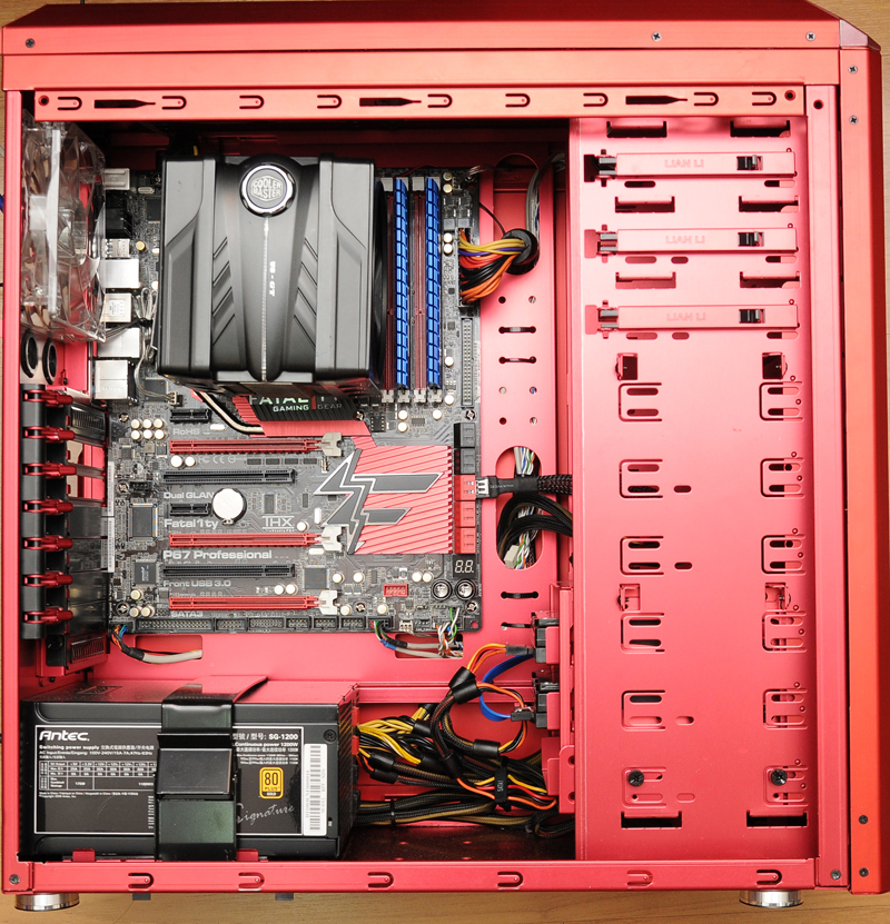
http://pic.xfastest.com/elvis/XF-VGA/XF-VGA-Bench-01.jpg
CPU: Intel Core i7-2600K OC @ 4.8GHz
Cooler: CoolerMaster V6-GT
Thermal Compound: Antec Formula 7
MB: ASRock Fatal1ty P67 Professional
Memory: Kingston HyperX T1 DDR3 @ 1600MHz 8-8-8-24
Power Supply: Antec SG1200W
Chassis: Lani-Li PC-P50R
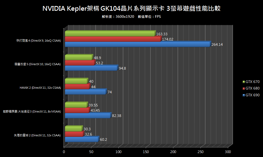
先來看採用NVIDIA Kepler架構 GK104晶片的顯卡使用3螢幕運行遊戲
並且特效全開的狀態下性能比較
http://picx.xfastest.com/elvis/Graphic/NVIDIA/GeForce/GTX670/Surround.png
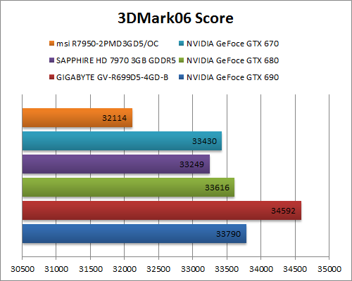
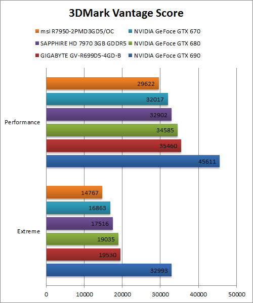
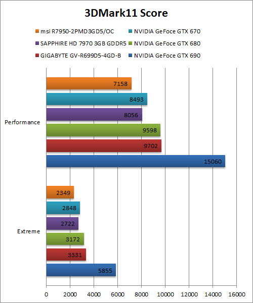
與競爭對手的比較
3DMark06 (DirectX 9)
http://picx.xfastest.com/elvis/Graphic/NVIDIA/GeForce/GTX670/DX9.png
3DMark Vantage (DirectX 10)
http://picx.xfastest.com/elvis/Graphic/NVIDIA/GeForce/GTX670/DX10.png
3DMark11 (DirectX 11)
http://picx.xfastest.com/elvis/Graphic/NVIDIA/GeForce/GTX670/DX11.png
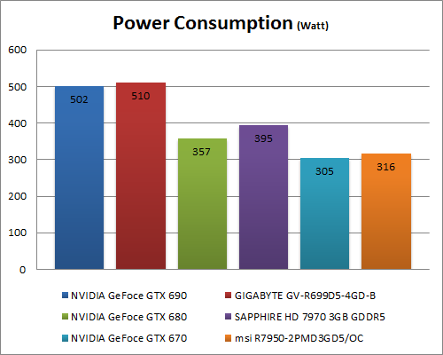
總結
綜合以上測試不難發現GeForce GTX 670相較於競爭對手同樣價位等級的Radeon HD 7950
無論是在性能或是功耗方面都略勝一籌,
在DirectX 11的效能甚至壓過對手目前最高階的HD 7970 !!
GeForce GTX 670 官方定價為US$399,
NVIDIA的策略是打算讓各個板卡商自行設計Layout,
因此在發行首波時段市面上應該就可以看到不少超頻版本的產品。
雖說NVIDIA在Kepler架構放棄了部分GPGPU通用運算的效能,
但也因此省下了更多功率消耗,創造更高的能源效率,
也符合絕大多數遊戲玩家的性能需求!
http://picx.xfastest.com/elvis/Graphic/NVIDIA/GeForce/GK104/02.jpg
--
推
08/10 19:09,
08/10 19:09
--
※ 發信站: 批踢踢實業坊(ptt.cc)
◆ From: 114.36.55.7
※ 編輯: ChangElvis 來自: 114.36.55.7 (05/10 21:23)
推
05/10 21:23, , 1F
05/10 21:23, 1F
→
05/10 21:35, , 2F
05/10 21:35, 2F
推
05/10 21:46, , 3F
05/10 21:46, 3F
推
05/10 22:05, , 4F
05/10 22:05, 4F
→
05/10 22:16, , 5F
05/10 22:16, 5F
推
05/10 22:16, , 6F
05/10 22:16, 6F
→
05/10 22:30, , 7F
05/10 22:30, 7F
→
05/10 22:41, , 8F
05/10 22:41, 8F
推
05/10 22:51, , 9F
05/10 22:51, 9F
推
05/11 00:30, , 10F
05/11 00:30, 10F
推
05/11 02:23, , 11F
05/11 02:23, 11F
推
05/11 21:19, , 12F
05/11 21:19, 12F